Title: A New Switching Algorithm Based On Single Phase Modulator for Z-Source Inverters With Reduced Computation Time and Enhanced Output Voltage

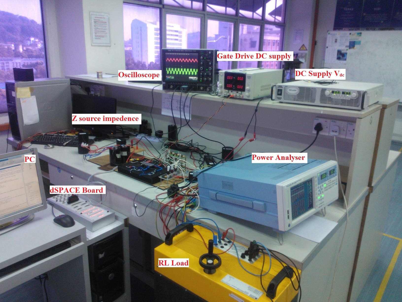
The inverter is one of the most common power electronics device used in industrial application. The main objective of the inverter is to produce an ac output waveform from a dc source. The main drawback of VSI is that the maximum output voltage obtained can never exceed the dc-link voltage. To obtain an output voltage higher than the input, an additional stage of dc/dc converter is required, which increases the cost of the system and decreases the efficiency. Recently, Z-source inverter (ZSI) is introduced to overcome the aforementioned disadvantages of VSI where a unique impedance network is coupled between the dc power source and the inverter main circuit. The obtained efficiency is higher due to the main feature of ZSI, which combines the advantages of buck/boost in one stage power conversion. Moreover, the reliability is improved due to the inclusion of the shoot-through (ST) interval, which is not allowed in VSI because it destroys the switching devices. The operation of ZSI has an additional ST state to boost the dc-link voltage besides the eight switching states in conventional converters, i.e. six active and two null vectors. This study proposes a new unified control method for the Z-source inverter family (ZSI), also called the One Dimension for Z-Source Inverters (ODZSI) based on the Single-Phase Modulator technique. The attractiveness of the modulation method lies on its extreme simplicity. A simple mathematical model is necessary to develop the ODZSI, and the calculations relative to switching sequence and the duty-cycles determination are highly simplified. The ODZSI is proposed to modulate single-phase H-bridge ZSI. Then, the same concept is extended to modulate three-phase qZSI/ZSI. In addition, the ODZSI can be used to control different impedance-source topologies. To achieve a maximum voltage gain, the ODZSI-MBC_3 is proposed. The shoot-through period is maximized by turning ON all the switches during the zero states, while iii the active states are kept unchanged. The obtained results using the ODZSI-MBC_3 are compared with those obtained with the carrier-based maximum boost control (CB-MBC), showing that the output voltage quality is enhanced with reduced computation burden. In order to reduce the switching losses, the ODZI-MBC_1 is also proposed. By using a carefully selected shoot-through states, the number of the switching transition is significantly decreased as each switch is locked to the positive or negative dc-rail during a period of 2π⁄3. Only two switches of the same leg will turn ON during the shoot through and the three ST times are distributed per two legs per control cycle. Additionally, as compared with space vector techniques, the inverter power losses are decreased, and the total execution time is reduced by 45%. The obtained results ensure the feasibility and validate the performance of the ODZSI. Moreover, due to the simple structure of the proposed control scheme and the reduced total execution time, it can be easily implemented on a slow and cheap controller. The presented concepts have been verified in simulations using Matlab/Simulink and validated experimentally.
Last Update: 22/11/2022